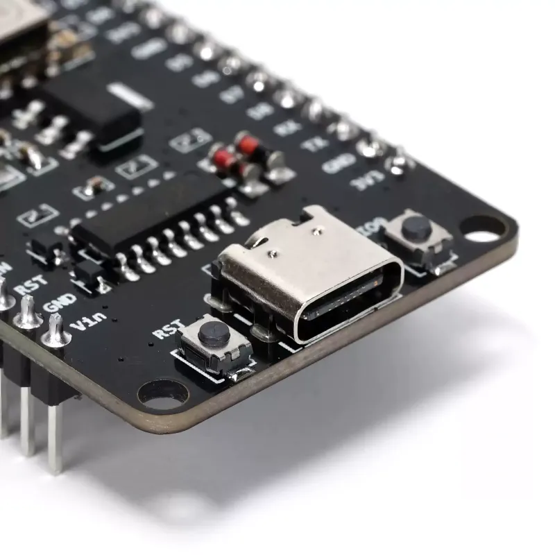
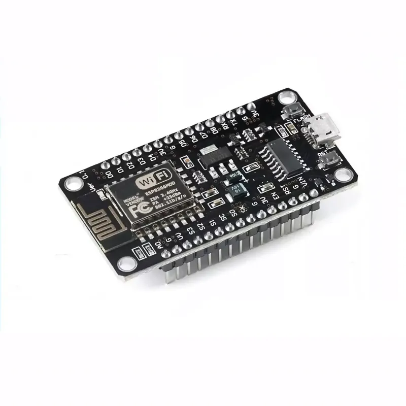


Product Description
Brand new NodeMCU, pre-flashed with
the latest firmware
(2015-07-04) — ready for use as soon as
it’s connected to a computer.
DE(GPIO16) can onLy binterrupt supported,
no pwm/i2c/ov
Label | PIN | Wiring pins for the ESP8266 development board | Pin Description |
1 | vCC | 3v | Power Supply (Positive) |
2 | GND | G | Power Supply (Ground) |
3 | GND | - | Power Supply (Ground) |
4 | NC | - | Undefined; reserved (no connection required) |
5 | NC | - | Undefined; reserved (no connection required) |
6 | LED | D4 | LCD Backlight Control Pin (connect to 3.3V if control is not required) |
7 | CLK | D5 | LCD SPI Bus Clock Pin |
8 | SDI | D7 | LCD SPI Bus Clock Pin |
9 | RS | D3 | LCD Register/Data Selection Control Pin |
10 | RST | D2 | LCD Reset Control Pin |
11 | cs | D1 | LCD Chip Select Control Pin |
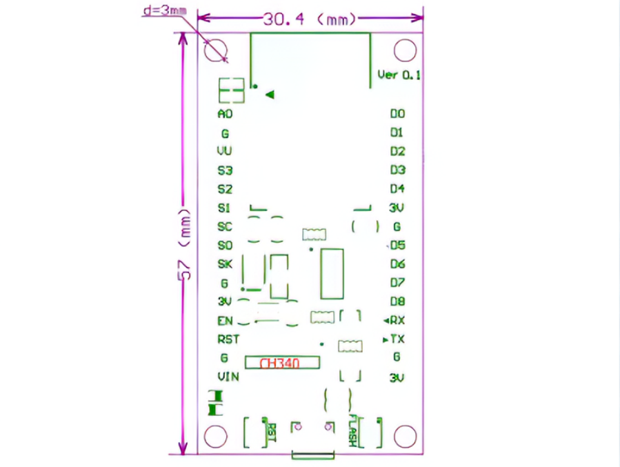
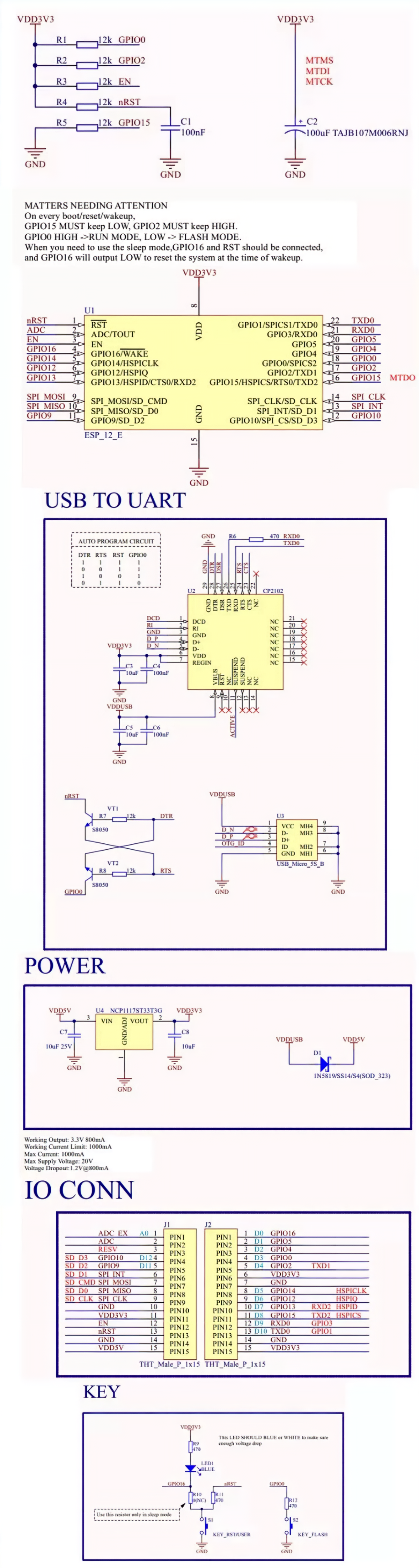
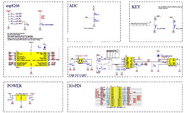
Nodemcu v3-CH340 sch
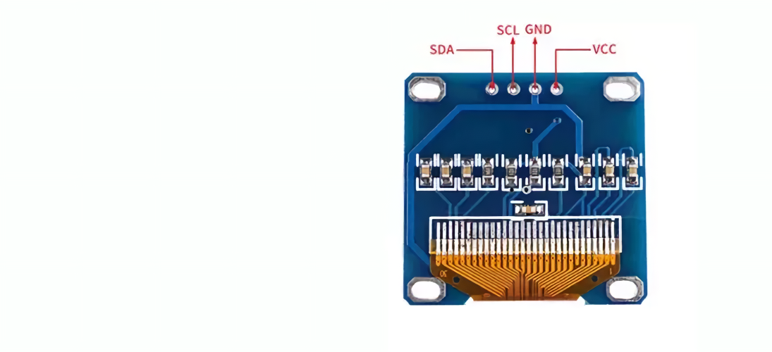
Pin definitions:
1. VCC: Positive power supply (3.3V–5V).
2. GND: Negative power supply (ground).
3. SCL: Clock signal line.
4. SDA: Bidirectional data line.
Brand new NodeMCU, pre-flashed with
the latest firmware
(2015-07-04) — ready for use as soon as
it’s connected to a computer.
DE(GPIO16) can onLy binterrupt supported,
no pwm/i2c/ov
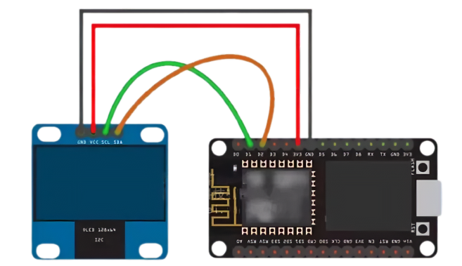
Demonstration of connecting an ESP8266 development board to a 0.96-inch OLED display (showing white text/graphics):
OLED Nodemcu
GND-----------GND
VCC-----------3V3/5V
SCL-----------D1(GPIO5)
SDA----------D2(GPIO4)
Product parameters
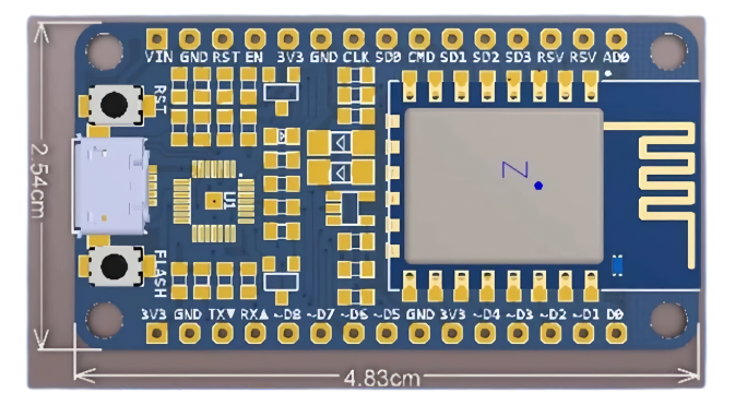
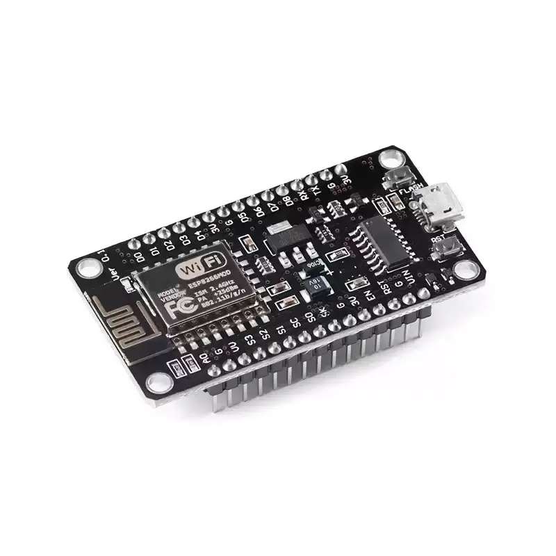
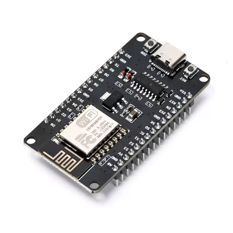
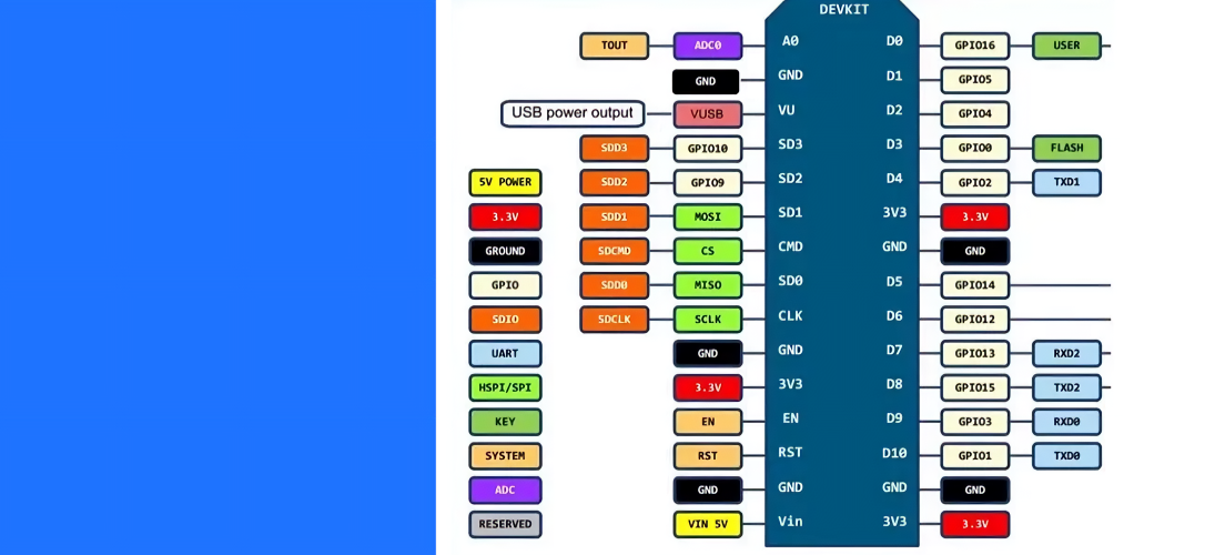
Pin Descriptions
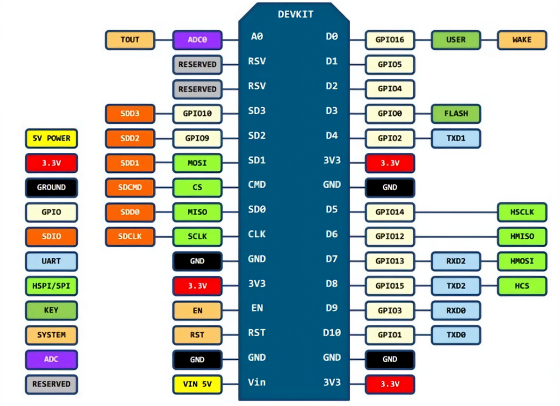
De(GPI016) can only be used as gpio read/write, no interrupt supported,no pwm/i2c/ow supported.
| Name | Function | direction |
ADO | Analog level sampling | enter |
RSV | reserve | - |
SD2 | GPIO | Input/Output |
SD3 | GPIO | Input/Output |
SD1 | SPI INT | - |
CMD | SPI MOSI | - |
SDO | SPI MISO | - |
CLK | SPI CLK | - |
EN | Chip Enable | Input |
RST | ESP12E Reset | Input |
DO | Number 10 | Input/Output |
D1~8 | Digital I/O with PWM functionality | Input/Output |
3V3 | 3.3V | - |
GND | land | - |
VIN | Power supply 4.5–9V | Input |
RX | UART Reception | Input |
TX | UART Output | Output |
2. Please maintain sufficient clearance around the antenna on the development board; otherwise, antenna performance may be compromised.
3. When the development board is connected to a computer via the USB port, plugging or unplugging other USB peripherals may cause the board to reset if the serial port is not currently open. This issue occurs only when the board is powered by the computer and the serial port is closed; it does not happen if the board is powered by a standard USB power adapter or if the serial port is already open.
4. If the GPIO0 pin is at a low logic level during power-up, the development board will enter firmware-flashing mode, and the user's program will not execute. If the board fails to operate correctly after power-up, please check the logic levels of the following pins: GPIO0 (High), GPIO2 (High), EN (High), RST (High), and GPIO15 (Low). If the levels do not match these requirements, please inspect and correct the peripheral circuitry.
5. If the firmware-flashing process is interrupted—resulting in an incomplete program—the board may fail to enter its normal operating mode. In such cases, hold down the "FLASH" button while connecting the USB cable to restore the ability to flash the firmware.
6. To use the sleep (deep sleep) function, you must connect the RST pin directly to the GPIO16 pin. You can make this connection manually or by soldering a 0-ohm resistor at the position marked "R3" on the development board. Note that once the sleep function is enabled, GPIO16 cannot be used for other purposes.
7. GPIO16 does not support interrupts, PWM, I2C, or One-Wire protocols; it can only be used as a standard general-purpose input/output (GPIO) pin.
8. Do not supply a voltage exceeding 5V to the development board, and do not connect the board's GPIO pins directly to peripherals operating at 5V logic levels. If such a connection is necessary, a level-shifting circuit must be used; otherwise, the board may suffer irreversible damage.