


Summary: On November 6, Diamond Foundry announced the production of the world's first 200 mm (approximately 7.9-inch) continuous single-crystal diamond wafer. The wafer delivers a thermal conductivity of approximately 2,000 W/m·K, several times higher than copper. Although the sample remains unpolished and is not yet ready for semiconductor manufacturing, the achievement demonstrates the feasibility of wafer-scale single-crystal diamond production, potentially opening a new path to solving thermal bottlenecks in high-performance AI chips.
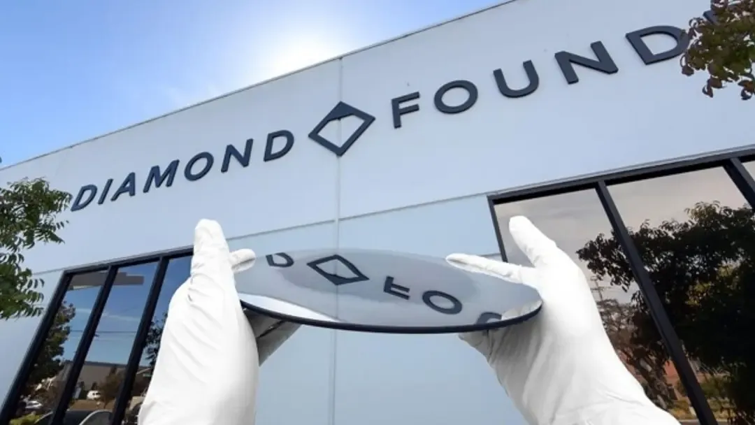
First-ever D200mm single-crystal diamond (as grown, unpolished) outside of Diamond Foundry’s South San Francisco headquarters.
As AI computing power continues to grow, localized hotspots inside semiconductor chips have become a major constraint on performance. Traditional metal-based cooling materials and polycrystalline diamond heat spreaders are approaching their performance limits, while single-crystal diamond has long been regarded as a promising next-generation thermal substrate.
The most important aspect of this breakthrough is its continuous single-crystal structure. Most commercially available 8-inch diamond heat spreaders are polycrystalline, containing numerous grain boundaries that impede heat transfer. By contrast, the new 200 mm sample consists of one continuous crystal, with an ordered carbon atomic lattice throughout and no grain boundaries between individual crystal grains. Both grain boundaries and structural defects can hinder thermal and electrical transport. A continuous single-crystal structure therefore offers a better opportunity to fully exploit diamond's exceptional thermal conductivity and electrical insulation properties.

High-purity single-crystal diamond has a room-temperature thermal conductivity of approximately 2,000 W/m·K, substantially higher than that of copper. In advanced semiconductor packaging, it could serve as a heat-spreading layer or substrate, rapidly distributing concentrated heat from GPUs and high-performance computing (HPC) chips. This could lower peak junction temperatures, reduce thermal throttling and ease the cooling requirements of entire systems. Diamond also has an ultra-wide bandgap of approximately 5.47 eV, making it theoretically suitable for high-voltage power devices and high-frequency radio-frequency (RF) applications.
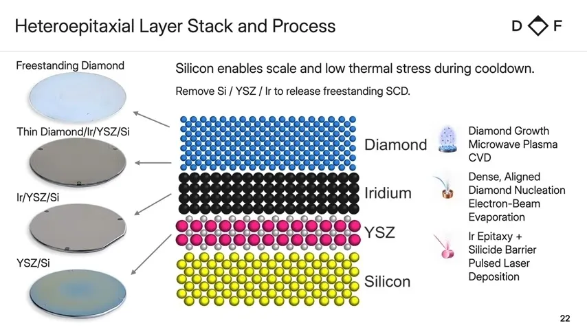
The main challenge in growing large-area continuous single-crystal diamond is not simply producing diamond, but maintaining lattice stability across an increasingly large surface. The leading approach is microwave plasma chemical vapor deposition (MPCVD). Throughout the deposition process, even minor fluctuations in plasma distribution, temperature fields or gas composition can introduce dislocations and structural defects. Once defect density exceeds acceptable levels, the material's thermal and electrical performance can deteriorate significantly. Although high-pressure, high-temperature (HPHT) synthesis is a well-established technique, scaling it to wafer-sized single crystals remains extremely difficult.
It is important to distinguish this achievement from a production-ready semiconductor wafer. The diamond crystal has only recently been removed from the growth reactor and has not yet undergone polishing. To meet semiconductor manufacturing standards, it must still pass several stages, including precision polishing, thickness uniformity control, full-wafer defect inspection, and thermal and electrical characterization. Manufacturers must also demonstrate consistent and repeatable growth across multiple production runs while resolving compatibility issues with existing semiconductor processes and other substrate materials. Another longstanding challenge is diamond's difficult-to-control doping process. Consequently, near-term applications are more likely to focus on thermal management rather than replacing silicon in transistor manufacturing.
Looking ahead, successful production at 200 mm provides a technical foundation for exploring 300 mm (12-inch) single-crystal diamond wafers, with a potential development target before 2030. Since 12-inch wafers are the mainstream format for advanced logic chip manufacturing, achieving stable production at this scale would represent a major step toward qualifying single-crystal diamond for integration into mainstream semiconductor fabrication facilities.
From the perspective of the AI computing industry, the significance of this material breakthrough is not that it will immediately replace the silicon-based semiconductor ecosystem. Instead, it introduces a potentially important new option at the advanced packaging level. As chip power density continues to increase, relying solely on external water cooling or immersion cooling is becoming increasingly expensive and challenging. If wafer-scale single-crystal diamond can eventually achieve stable yields and commercially viable production costs, it could expand the thermal design limits of semiconductor packages, allowing higher sustained power consumption and operating frequencies to translate into greater computing performance.
In short, wafer-scale continuous single-crystal diamond has moved from a theoretical possibility to a physical demonstration, although substantial manufacturing challenges remain. If these challenges can be overcome, the material could become a key thermal management solution for handling localized hotspots in future high-performance AI chips.

